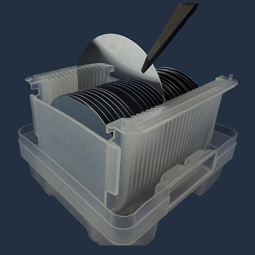
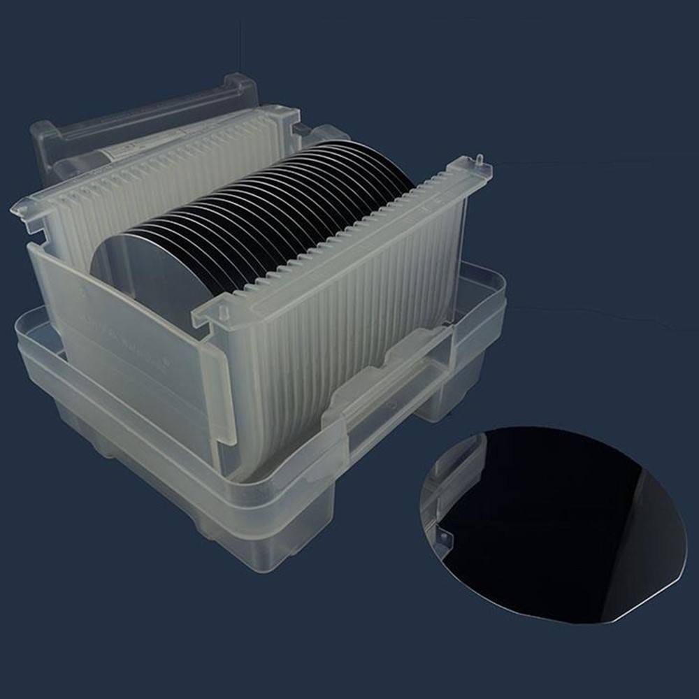
Monocrystalline Silicon Wafer Double Side Polished
We provide 100mm, 150mm, 200mm, 300mm, 450mm and other product grade silicon wafers. The model, resistivity, crystal orientation,thickness, etc. can be customized according to customer requirements.
Description
Description
Monocrystalline silicon wafers are thin, circular slices of single-crystal silicon that are widely used in the electronics industry to produce integrated circuits, solar cells, and other electronic components. Here are some of their features and packaging:
Features:
High Purity: Monocrystalline silicon wafers are made from a single, large crystal of high-purity silicon, which ensures that they have extremely low levels of impurities and defects.
Uniformity: The crystal structure of monocrystalline silicon wafers is highly ordered and uniform, which makes them ideal for use in electronic components where precise and predictable behavior is required.
Efficiency: Monocrystalline silicon wafers are highly efficient at converting light into electricity, which makes them ideal for use in solar cells.
Low Light-induced Degradation (LID): Monocrystalline silicon wafers exhibit very low LID when exposed to sunlight, which means that their performance does not degrade significantly over time.
Specification
|
Materials |
Optical Grade Silicon |
|
Purity |
>99.9999% |
|
Growth method |
FZ |
|
Type |
N or P |
|
Orientation |
<100> or <111> |
|
Resistivity |
>100 ohm.cm |
|
Transmittance |
>52.5% |
|
Oxygen Concentration(1/cm3) |
<1×10E16 |
|
Carbon Concentration(1/cm3) |
<1×10E15 |
|
Doping Element Concentration(1/cm3) |
<1×10E17 |
|
Coefficient of thermal expension |
2.5(T=300k) |
|
Linear Expension Coefficient |
(2-9)×10-6 k-1 |
|
Hardness, Mohs |
7.0 |
|
Density |
2.33g/cm3 |
|
Melting point |
1414℃ |
|
Dielectric Constant |
13 |


Packing
Protection: Monocrystalline silicon wafers are extremely delicate and brittle, and so they must be carefully handled and protected during packaging to prevent damage.
Cleanliness: The wafers must be packaged in a clean environment to avoid contamination, which could affect their performance.
Flatness: Monocrystalline silicon wafers must be packaged in a way that preserves their flatness and prevents warping or bending, which could affect their performance.
Anti-static: Packaging materials must be anti-static to prevent damage from electrostatic discharge.
Hot Tags: monocrystalline silicon wafer double side polished
Send Inquiry
You Might Also Like
